


六軸並聯機器人在VR眼鏡測試上的應用
來源: 作者: titan 發布時間: 2026-07-07 15:33 76 次瀏覽
VR眼鏡如何透過檢測減少暈眩感?
VR眼鏡(Virtual Reality Headset)核心:雖然 VR 眼鏡由顯示器、感應器和音訊設備組成,但其最核心的部分是由鏡頭和液晶顯示器(LCD)組合而成的「光學系統」,成像的效果直接影響了客戶的體驗。稍有不佳,就會造成頭暈、頭痛、目眩、視物傾斜變形,甚至影響到使用者的健康。在此設備的光路中,對調整精度和維度控制上都很高。六軸並聯機器人可以實現對鏡片品質的線上檢測,及時發現問題並採取措施,確保產品品質。將六軸並聯機器人整合到鏡片生產線中,實現鏡片測試、處理和組裝的自動化流程,提高生產效率和品質穩定性。透過六軸並聯機器人的應用,可以實現鏡片測試過程的自動化、高效化,提高生產效率和產品質量,同時減少人為操作的誤差和勞動強度。VR眼鏡主要測試:鏡片解析度測試、鏡片表面品質檢測、影像變形測試,都可以使用六軸並聯機器人來完成。鏡片解析度測試
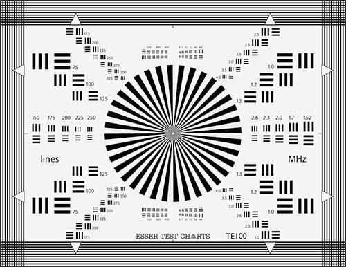
.高對比度測試圖案:通常選用棋盤格、網格或直線圖案,這類圖案具備清晰的邊緣,便於相機辨識細節與對比度。
.工業相機與穩定光源:相機作為測量工具記錄成像,而均勻穩定的光源則是避免產生反射干擾、確保測試結果準確的前提。
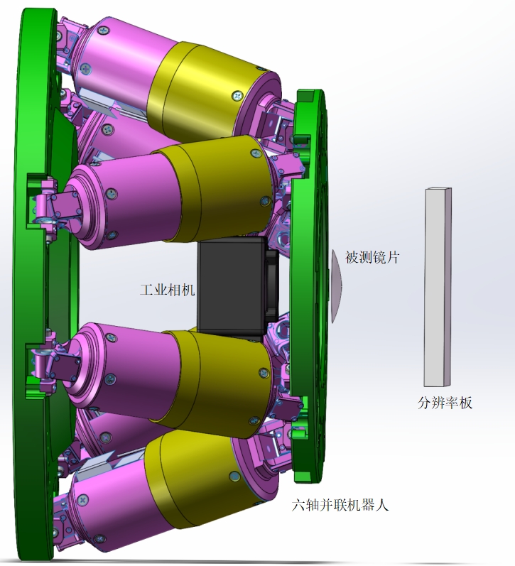
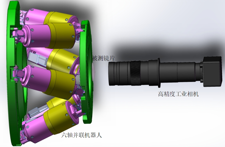
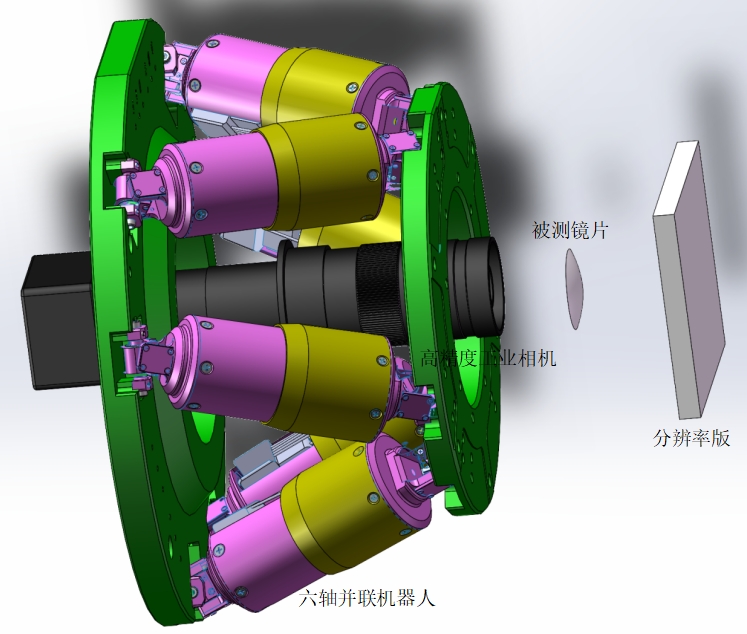
.六軸並聯機器人(調整機構):本方案中最關鍵的自動化設備。它具備六個獨立旋轉關節,利用其高重複定位精度來精確調整相機、鏡片與圖案之間的相對位置。
測試步驟
設定測試環境:將被測鏡片固定在六軸並聯機器人的台面上。同心放置在適當的位置,確保光線充足、均勻,避免反射和干擾。
選擇測試圖案:選擇合適的解析度測試圖案,並將其放置在適當的位置,以便鏡片能夠清晰顯示圖案的細節。
觀察成像:透過六軸並聯機器人帶動被測鏡片、在相機上成像解析度板的測試圖案。記錄成像的細節、清晰度和畸變。
記錄結果:記錄鏡片成像的情況,包括能夠清晰顯示的最小細節和分辨率,以及是否有畸變、色差等情況。
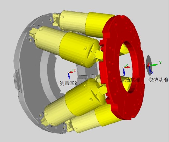
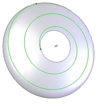
在測試過程中,被測鏡片的空間位置調整的基準,需要在鏡片的焦點之上。可以使用六軸並聯機器人的工具座標系的功能來實現。如下圖:
鏡片表面品質檢測
表面品質檢測主要評估鏡片的平整度、光滑度以及無瑕疵程度。這對於 VR 產品至關重要,因為光學系統是產品的核心,任何成像瑕疵(如氣泡、刮痕、污點)都可能導致使用者出現頭暈、頭痛或目眩等不適症狀。 檢測步驟
先清潔的測試鏡片。將鏡片固定在六軸並聯機器人的檯面上。再使用高分辨工業相機在鏡片的表面成像,來監測表面品質。透過影像對鏡片表面進行全面檢查,包括平整度、光滑度和瑕疵(如氣泡、刮痕、污點等)。在檢測的過程中,機器人要帶動鏡片。沿著鏡面表面移動,掃描整個鏡片曲面。
基本光路
掃描軌跡
 這種運動軌跡可以用運行方案的中的座標系轉換功能來實現。
影像畸變測試
影像畸變測試是指透過放置被測圖案在鏡片前,觀察圖案是否出現彎曲或扭曲,以檢驗光路的畸變。 VR眼鏡的整體光路如下。
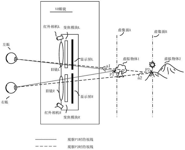 在測試過程中,要模擬眼球在光路中的動態位置。檢驗在不同的眼神角度下,成像的清晰度。
測試步驟
設定測試環境:將鏡片放置在適當的位置,確保光線充足、均勻,避免反射和干擾。
選擇測試圖案:選擇合適的變形測試圖案,並將其放置在適當的位置,以便鏡片能夠清晰顯示圖案的直線或曲線。
觀察成像:透過六軸並聯機器人帶動工業相機觀察鏡片成像測試圖案,注意觀察圖案的直線或曲線是否呈現扭曲或形變。
記錄結果:記錄鏡片成像的情況,包括是否有徑向畸變(影像中心的直線是否彎曲)和切向畸變(影像邊緣的直線是否彎曲)等情況。
分析結果:根據觀察和記錄的數據,評估鏡片的畸變性能,確定鏡片是否符合要求。
基本光路:
最新消息
3
UA-24279210-1---


服務熱線:886-2-2655-2200 業務咨詢:151 / 維修校正:185
產品
文章
搜索
名稱描述內容
【關鍵字搜索】:
請於欄位下方先點選"內容"
當前位置: